Work on two-dimensional materials continues to yield both surprises and new devices.
Fifteen years ago next month, Konstantin Novoselov, Andre Geim and colleagues published the paper ‘Electric field effect in atomically thin carbon films’ in Science and kick-started research into the two-dimensional material graphene 1 . Much has happened since: a Nobel Prize in Physics in 2010 for Novoselov and Geim, and the launch of the €1 billion Graphene Flagship programme in Europe in 2013, to start; not to mention the rich physics and diverse potential applications. And the surprises keep coming: last year, for example, unconventional superconductivity was observed in samples of twisted bilayer graphene 2 .

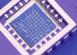
A packaged and wire-bonded die containing 64 nanoelectromechanical accelerometers made from suspended double-layer graphene ribbons with attached silicon proof masses. Credit: Springer Nature Ltd
The paper itself begins with a discussion of electronics and the approaching performance limits of silicon-based technology, but concludes “nontransistor applications of this atomically thin material ultimately may prove to be the most exciting”. Graphene is a semimetal and lacks an energy bandgap. Building devices that can actually switch off is thus a problem. Nevertheless, methods to open a bandgap have been established, such as forming graphene nanoribbons, and efforts to create a sizeable bandgap in the material and build digital logic devices continue 3 .
Key to the success of graphene is its range of remarkable properties, from high electron mobility and mechanical strength to transparency and flexibility. This, in turn, is reflected in its range of potential applications, from electrodes for supercapacitors 4 to membranes for water desalination 5 and from flexible electronics to spintronic devices 6 . The diversity of applications is further highlighted in this issue of Nature Electronics, where Xuge Fan and colleagues show that graphene can be used to build transducers for nanoelectromechanical accelerometers (pictured).
Such accelerometers could be used in wearable devices to monitor activity levels. However, they require transducers that are ultra-small and sensitive. The researchers — who are based at institutes in Sweden and Germany — create their transducers by attaching silicon proof masses to suspended double-layer graphene ribbons. The approach leads to accelerometers that occupy at least two orders of magnitude smaller die area than conventional state-of-the-art silicon accelerometers. Notably, the devices are fabricated using processes that are compatible with large-scale semiconductor manufacturing technologies.
The impact of the 2004 paper from Novoselov, Geim and colleagues also extends beyond the properties and applications of graphene — the work has, in particular, inspired the search for other two-dimensional materials. Today, an array of single-layer materials, which have a corresponding array of electronic behaviours, is available: from the wide-gap insulator hexagonal boron nitride to the semiconductor molybdenum disulfide to the ferromagnet chromium triiodide. Furthermore, different two-dimensional materials can be stacked on top of each other to create layered structures known as van der Waals heterostructures. This approach has led to the design of devices such as transistors 7 , memristors 8 , photodetectors 9 and light-emitting diodes 10 .
In many areas, fabrication issues remain a barrier to practical devices. For applications in flexible and wearable electronics, solution processing is an important requirement. Certain two-dimensional nanosheets can be dispersed in solvents as stable colloidal inks and then assembled into continuous thin films in which neighbouring sheets interact via van der Waals forces. In a Perspective elsewhere in this issue, Zhaoyang Lin, Yu Huang and Xiangfeng Duan at the University of California, Los Angeles explore the development of these solution-processable van der Waals thin films and their use in high-performance large-area electronics.
Essential to this approach is the availability of high-quality two-dimensional nanosheets that can be readily dispersed in solution to form the inks. The researchers thus first consider the production of nanosheet inks with the required range of electronic properties — from insulating to semiconducting to metallic — using both bottom-up synthesis and top-down exfoliation methods. They then examine the scalable assembly of the nanosheets into thin films, which can be achieved with techniques such as spin coating, layer-by-layer assembly and ink-jet printing. Finally, they highlight the preliminary devices and integrated circuits built with the approach to date and assess their future application in wearable electronics.